A printed circuit board (PCB) mechanically supports and electrically connects electronic components using conductive tracks and pads etched from copper sheets laminated onto a thin non-conductive substrate. All the electronic components such as capacitors, resistors or diodes are soldered on the PCB with a low melting flux heated by a Soldering Iron.
Advancement in the PCB fabrication mechanisms along with VLSI (Very Large Scale Integration) is one of the big reasons why we can today hold engineering marvels like laptops, tablet PCs and very powerful mobile phones with huge computing capacity that are packed within a hand-holdable form factor.
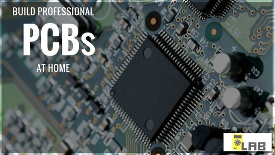
So lets quickly run through the steps to build professional quality PCBs right at your home and bring your circuit ideas to life.
1. CREATE A PCB LAYOUT:
We assume that you are well equipped with layout softwares like EAGLE and DIPTRACE. However, if you don’t know how to create a PCB layout from a schematic diagram, you can watch the video on Create a PCB Layout in as easy as 3 steps and come back to resume the process from here.
After having created the layout, the next step is printing the layout on a piece of paper. Industries usually use trace papers to print the layout. But I have tested that plane A4 size papers work better than trace papers for the process I follow at home. Trace papers give better results when you have all the industry equipments in place. Also note that the printer you use is a laser printer and not an inkjet printer. If you are not sure, you can use the print out from any photocopier.
The reason inkjet printers don’t work best is because the paper soaks the ink but in a laser printer the carbon particles are deposited at the surface and can be easily transferred onto the copper plate.
2. PRINTING ON THE COPPER PLATE:
The purpose of printing the layout on a paper is to transfer the traces (the lines in the layout are called traces) onto the copper layer. Traces are the copper lines that are required to stay back and the rest of the copper shall be removed from the board to expose the underlying non-conducting substrate. Essentially, this process has fairly simple objective i.e. to transfer the traces from the paper onto the copper plate. Here’s how I do it.
Take a small piece of sand paper and gently clean the copper surface with it. This basically serves three purposes.
- It removes any dirt or layer that might have formed as a result of storage over a long period of time or reactions with certain areal substances.
- It activates the copper and enables quicker reaction with Ferric Chloride (More on this in the next step)
- It makes the surface a bit rough which enables the carbon particles to stick quicker onto the copper film.
The next step is to put the paper on top of the copper film and provide a hot treatment so that the carbon is duly transferred over to the copper plate. I use an electric iron to rub it over the paper. You have to actually keep rubbing it over the paper with pressure and not just leave the iron onto paper. After rubbing it on the paper for almost 15 minutes, leave it to cool off for a while (5 minutes). Then rub off the paper as gently as you can with periodic application of water. This should be done very carefully and should take a bit of time. If done properly only traces should be left behind and rest of the paper is removed to expose the copper.
No matter how carefully you do it, there might be occasional off days, where all or some part of the trace is removed off as well. Don’t worry, its not time to scrap the board and restart yet!! You can use a good quality thin-nibbed permanent marker to draw out the traces that didn’t come off.
Alternatively, there might be also occasions when two traces are very close and the paper from with in the traces are not completely removed. Removing the paper from the gaps is a vital process and I prefer a small pocket knife to carefully take off the unwanted paper traces. Even a thinnest left out copper trace can cause short circuits. So this has to be done with a lot of care.
3. ETCHING:
Etching is a chemical process that is used to remove the unwanted copper from the non-conducting substrate. Etching is done with a chemical Ferric Chloride which is easily available at a chemical dealer. Mix one part of Ferric Chloride to 5 parts of water and steer the solution with a glass rod. Make sure to use plastic containers for creating the solutions as metals will corrode due to effect of Ferric Chloride. You will notice a that the water heats up a bit which is normal. Please use gloves and dont touch the solution with your bare hands and take care not to spill it in your dress else that will be the last time you wear that shirt!! (I damaged my then favorite shirt in the initial days 🙁 ). Once the chemical is properly mixed with water, drop the PCB in the solution. Don’t leave the solution in a static state. Make sure to nudge the container every now and then to speed up the etching process. The etching process takes anything between 10 minutes to 30 minutes (depending on the size of the PCB and quality of Ferric Chloride powder).
After being completely satisfied that the exposed copper has been removed, proceed to the next step.
NB: (For the Theoritical Geeks) For me etching has always been a process to remove unwanted copper from the non-conducting substrate. However, if you are one of those who believe more in the hows than the whats and whys (No, I am not judging you), here is how the chemical process works:
2FeCl3 + Cu → 2FeCl2 + CuCl2
4. DRILLING:
In industrial PCB Design, drilling is done before etching. However, if you follow my procedure; which is completely without the industry tools (not to say they are damn expensive!!), I have found better results with etching first and then drilling. Let me explain. In case of industrial design the process of printing the layout onto the PCB is far more superior, effective and the carbon-content of the coating is more; which makes the carbon to stick better onto the surface of the PCB. However, the process that we follow is not as robust. So when we drill first and then etch, then chances are that the drill would have removed a bit of coating around the areas of the pads (where the terminals are soldered on the board). This would further lead to bad quality soldering, decreases circuit longevity, and sometimes causes sparking in case of higher voltages.
Most of the components in basic electronics can be soldered comfortably with a 0.80mm diameter drilling bit. However, there might be certain elements that require a hole of 1mm diameter which can be achieved by a drilling bit of 1mm. Advanced users would sometimes require drills of various shapes and diameters (example being that of a relay, VGA port, etc).
5. SOLDERING:
I have always believed soldering to be an art. It requires lot of practice to master the art of soldering and the only way to be perfect in the art is to just put your head down and practice as much as you can. Having said that, there are certain things that helps in avoiding hazards during soldering.
a) Dont expose your naked eyes directly to the fume of the soldering iron. They can cause irritation and reddening of the eyes. A pair of glasses with white lens should do fine to keep the fumes away.
b) Invest in a good quality soldering station that has a fan to suck the smoke, regulator to control the temperature of soldering iron (as certain ICs are very sensitive to heat).
c) Make sure to apply the solder at the base of the board. This lead to better quality soldering.
d) In case of contact with the skin, rinse the affected area with cold water and apply any ointments after consultation (if the burns are major).
Once the process of soldering is complete, you can use a clipper to clip the remaining metals terminals from the tip of the solder. In certain cases the soldering loosens after clipping. Make sure to fix those by a quick touchup with the soldering iron.
6. TESTING:
This is a fairly simple and obvious step. You will need a good quality multimeter and a connectivity tester (yes you can test connectivity in a multimeter, but these led powered devices cost only around 50 bucks and helps in quicker detection of probable short circuits of disconnections). After making sure that all the connections are as required, connect the circuit to the power source. If this is your first PCB then its better to be sure than to be sorry as a minute short circuit can ruin all elements and hard work you did to reach here. If you circuit works fine (I wish it does 🙂 ), bravo!! You made it.
Congratulations on your first home-made circuit and welcome to a world of excitements and adventures you will have as a electronics hobbyist. I am not sure, if I should be making a video lesson to show how to design a PCB at home. If you want the video lesson let me know in the comments below. Thanks for reading.


4 Comments
I truly enjoy looking through on this web site , it holds superb content .
hi that pst so interesting
yo this pst very interesting
Appreciating the hard work you put into
your website and detailed information you present. It’s great to
come across a blog every once in a while that isn’t the same outdated rehashed
information. Wonderful read! I’ve bookmarked your site and I’m
adding your RSS feeds to my Google account.